All Images
News Release 08-132
The Shape of Things to Come
Flexible web of micro-sensors enables eye-shaped camera, heralds new class of electronics technology that can conform to almost any shape
This material is available primarily for archival purposes. Telephone numbers or other contact information may be out of date; please see current contact information at media contacts.

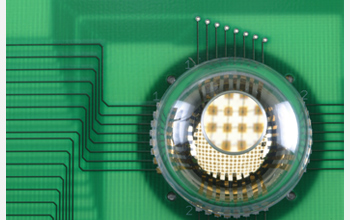
The electronic-eye camera developed by researchers from the University of Illinois at Urbana-Champaign and Northwestern University. The array of pixels is visible through the magnified image created by the lens.
Credit: Beckman Institute, University of Illinois
Download the high-resolution JPG version of the image. (900 KB)
Use your mouse to right-click (Mac users may need to Ctrl-click) the link above and choose the option that will save the file or target to your computer.
John Rogers of the University of Illinois at Urbana-Champaign describes the new camera he helped develop that is based on the structure of the human eye. Rogers explains the idea behind the camera, how it is crafted, the benefits of the device over existing cameras, and how the same technology can be used for a range of devices, including flexible sensors and prosthetics.
Credit: University of Illinois at Urbana-Champaign/Northwestern University/National Science Foundation
Yonggang Huang of Northwestern University describes the new retina-like camera sensor and how a careful study of the properties of materials allowed the team to move beyond the rigid, planar camera chips common in today's digital cameras and instead create a flexible array of photosensitive pixels.
Credit: University of Illinois at Urbana-Champaign/Northwestern University/National Science Foundation

This color picture of an eye is an actual image obtained with the new 256-pixel electronic eye camera. The curved surface rendering at the top corresponds to the image extracted directly from the camera, while a planar projection of the image appears below.
Credit: Beckman Institute, University of Illinois
Download the high-resolution JPG version of the image. (1.1 MB)
Use your mouse to right-click (Mac users may need to Ctrl-click) the link above and choose the option that will save the file or target to your computer.

This image, captured during the electronic eye fabrication process, shows a silicon focal plane array (dark brown) and electronics on a hemispherical transfer element (translucent).
Credit: Beckman Institute, University of Illinois
Download the high-resolution JPG version of the image. (2.8 MB)
Use your mouse to right-click (Mac users may need to Ctrl-click) the link above and choose the option that will save the file or target to your computer.

Low magnification scanning electron micrograph of a collection of silicon photodetector pixels and electronics interconnected by arc-shaped ribbons, on a hemispherical substrate. These interconnects bow upward to accommodate the large mechanical strains needed to transform the planar layouts in which the systems are initially fabricated to the hemispherical geometries needed for implementation in the electronic eye. The image is colorized: pixel elements and interconnects appear gold; the substrate appears light blue.
Credit: Beckman Institute, University of Illinois
Download the high-resolution JPG version of the image. (1.3 MB)
Use your mouse to right-click (Mac users may need to Ctrl-click) the link above and choose the option that will save the file or target to your computer.

This high magnification scanning electron micrograph shows a small cluster of silicon photodetector pixels and electronics interconnected by arc-shaped ribbons, all on a hemispherical substrate. These interconnects bow upward to accommodate the large mechanical strains needed to transform the planar layouts in which the systems are initially fabricated to the hemispherical geometries needed for implementation in the electronic eye. The image is colorized: pixel elements and interconnects appear gold; the substrate appears light blue.
Credit: Beckman Institute, University of Illinois
Download the high-resolution JPG version of the image. (1.3 MB)
Use your mouse to right-click (Mac users may need to Ctrl-click) the link above and choose the option that will save the file or target to your computer.

This image shows a close-up view of the silicon photodetector pixels and electronics interconnected by arc-shaped ribbons. The scale bar represents 10 micrometers (millionths of a meter).
Credit: Northwestern University and University of Illinois
Download the high-resolution JPG version of the image. (108 KB)
Use your mouse to right-click (Mac users may need to Ctrl-click) the link above and choose the option that will save the file or target to your computer.
